
- Dit onderwerp bevat 0 reacties, 1 deelnemer, en is laatst geüpdatet op 3 januari 2022 at 17:28 door Anna.
-
AuteurBerichten
-
-
3 januari 2022 om 17:28 #7309Anna@akrasko97
Koolstofnanobuis
allotroop van koolstof in cilinder-/buisvorm
Bron: https://artigos.wiki/blog/nl/Nanotube
Koolstofnanobuizen (Engels: carbon nanotubes of CNT) zijn een van de allotropen van koolstof en onderdeel van de groep fullerenen. Een koolstofnanobuis is een opgerolde laag grafeen, hol vanbinnen, waarbij de lengte tienduizenden malen groter kan zijn dan de diameter. Koolstofnanobuizen hebben veel interessante eigenschappen waardoor zij geschikt zijn voor een breed scala aan toepassingen, onder andere in nanotechnologie, elektronica, optica en nieuwe materialen.
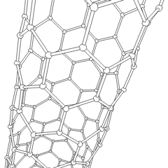
Enkelwandige Koolstofnanobuis
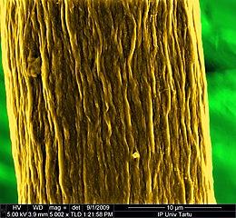
Een rasterelektronenmicroscopische opname van een vezelbundel bestaande uit Koolstofnanobuizen
Ontdekking
Veel wetenschappelijke artikelen noemen Sumio Iijima als de ontdekker van koolstofnanobuizen. Hij schreef in 1991 een artikel[1] in Nature waarin hij de aanwezigheid van holle structuren van koolstof beschreef, in roet ontstaan bij het vonken van een koolstof elektrode. Hoewel het onderzoek naar koolstofnanobuizen pas sinds het artikel van Iijima op gang is gekomen zijn er eerdere foto’s van koolstofnanobuizen bekend uit een Russisch natuurkundig tijdschrift, in een artikel van Radushkevich en Lukyanovich. In die tijd was de communicatie tussen wetenschappers in het westen en de Sovjet-Unie echter beperkt, wat mogelijk de oorzaak was dat het artikel niet echt in de westerse wetenschap is doorgedrongen.… verder over types, structuur en synthese. En het gaat over eigenschappen en toepassingen. Naast elektrische, thermische en mechanische eigenschappen worden ook medisch-biologische eigenschappen beschreven:
Medisch-biologische eigenschappen
Met name de langere nanobuizen worden ervan verdacht in het lichaam soortgelijke eigenschappen te vertonen als asbest: ze veroorzaken chronische irritatie doordat ze niet of nauwelijks afgebroken kunnen worden. Dat zou kunnen leiden tot asbestose.[12] Dat is in de eerste plaats een risico tijdens de productie van nanobuizen; uit de meeste producten met nanobuizen komen deze waarschijnlijk niet vrij tijdens normaal gebruik. Na afdanking van het product is het vrijkomen afhankelijk van de aard van de afdanking: vuilstort, verbranding, vergaan. (NB: Dat wordt dus nog een probleem!)Bij Toepassingen worden ook computertechnologie en “bacteriedoders” genoemd.
Bacteriedoders
Enkelvoudige koolstofnanobuizen (SW CNT) blijken in een onderzoek van een team rond M. Elimelech effectief bij het doden van de bacterie E. coli. Vermoedelijk prikken de buisjes door de celwanden van de bacteriën. Meerwandige koolstofnanobuizen zijn minder effectief.[15] De giftigheid van SWCNT’s was eerder ook al vastgesteld in de longen van muizen, al kan hier volgens Elimelech vervuiling met zware metalen een rol hebben gespeeld.[16][17]Computers
Onder leiding van Max Shulaker heeft een onderzoeksteam van de Stanford-universiteit in Californië in 2013 een eenvoudige, functionerende computer weten te bouwen, bestaande uit 178 transistoren op basis van koolstofnanobuizen.[18] Deze machine kan simpele berekeningen maken en draait op een besturingssysteem en programmatuur uit de jaren–’80.[19][20]Inmiddels zijn onderzoekers aan MIT erin geslaagd de transistoren onder fabrieksomstandigheden te maken met dezelfde faciliteiten als gebruikt worden voor silicium-chips, zodat de productie van deze computer voor de markt op relatief korte termijn gerealiseerd kan worden.[21]
==========================================================
Oke, dus het wordt met deze technologie al langer geexperimenteerd. De nanobuisjes zijn heel dun, het wordt genoemd: 25 duizend keer dunner dan menselijk haar.
Die nanobuisjes kunnen dus hele lange buisjes zijn en ze kunnen al transistor, geleider, gebruikt worden. In computertechniek biedt het kansen om nog kleiner te gaan.
En als het lichaam ook een biologische computer is, dan wordt het ook volop geexperimenteerd daarin. En hadden we onlangs veelvoudig “grafeen” gehoord?
Nog een artikel uit ScietechDaily.com over deze technologie (Engels)
===================================
“Fundamental Discovery” Used To Turn Nanotube Into Tiny Transistor – 25,000x Smaller Than Width of a Human Hair
An international team of researchers has used a unique tool inserted into an electron microscope to create a transistor that’s 25,000 times smaller than the width of a human hair.
The research, published in the journal Science, involves researchers from Japan, China, Russia, and Australia who have worked on the project that began five years ago.
QUT Center for Materials Science co-director Professor Dmitri Golberg, who led the research project, said the result was a “very interesting fundamental discovery” which could lead a way for the future development of tiny transistors for future generations of advanced computing devices.
A designer view of a single-wall carbon nanotube intramolecular junction with metallic portions on left and right ends and a semiconductor ultrashort ~3,0nm channel in between. Credit: National University of Science and Technology, Moscow
“In this work, we have shown it is possible to control the electronic properties of an individual carbon nanotube,” Professor Golberg said.
The researchers created the tiny transistor by simultaneously applying a force and low voltage which heated a carbon nanotube made up of a few layers until outer tube shells separate, leaving just a single-layer nanotube.
The heat and strain then changed the “chilarity” of the nanotube, meaning the pattern in which the carbon atoms joined together to form the single-atomic layer of the nanotube wall was rearranged.
The result of the new structure connecting the carbon atoms was that the nanotube was transformed into a transistor.
Professor Golberg’s team members from the National University of Science and Technology in Moscow created a theory explaining the changes in the atomic structure and properties observed in the transistor.
Lead author Dr. Dai-Ming Tang, from the International Center for Materials Nanoarchitectonics in Japan, said the research had demonstrated the ability to manipulate the molecular properties of the nanotube to fabricate nanoscale electrical devices.
Dr. Tang began working on the project five years ago when Professor Golberg headed up the research group at this center.
“Semiconducting carbon nanotubes are promising for fabricating energy-efficient nanotransistors to build beyond-silicon microprocessors,” Dr. Tang said.
“However, it remains a great challenge to control the chirality of individual carbon nanotubes, which uniquely determines the atomic geometry and electronic structure.
“In this work, we designed and fabricated carbon nanotube intramolecular transistors by altering the local chirality of a metallic nanotube segment by heating and mechanical strain.”
Professor Golberg said the research in demonstrating the fundamental science in creating the tiny transistor was a promising step towards building beyond-silicon microprocessors.
Transistors, which are used to switch and amplify electronic signals, are often called the “building blocks” of all electronic devices, including computers. For example, Apple says the chip which powers the future iPhones contains 15 billion transistors.
The computer industry has been focused on developing smaller and smaller transistors for decades, but faces the limitations of silicon.
In recent years, researchers have made significant steps in developing nanotransistors, which are so small that millions of them could fit onto the head of a pin.
“Miniaturization of transistors down to nanometer scale is a great challenge of the modern semiconducting industry and nanotechnology,” Professor Golberg said.
“The present discovery, although not practical for a mass-production of tiny transistors, shows a novel fabrication principle and opens up a new horizon of using thermomechanical treatments of nanotubes for obtaining the smallest transistors with desired characteristics.”
-
-
AuteurBerichten
- Je moet ingelogd zijn om een antwoord op dit onderwerp te kunnen geven.